
I spend a lot of my time chasing bandwidth. Not the personal kind (although my calendar would appreciate more of that), but the physical bandwidth that moves bits across the infrastructure running the world’s AI models.
And lately, the trail has led me to light – literally. Optical chips, or photonic integrated circuits (PICs), use particles of light known as photons to carry and process information. This approach offers advantages such as higher bandwidth and speed compared to electronic chips that use electrons, enabling the development of energy-efficient optical computing and AI. This article covers the “why” I believe we should have our eyes on the optical chips.
The Gold Rush
Let’s travel back in time to the 19th century, when the so-called “gold rush” took place. If AI is today’s gold, then chip manufacturers are the shovel sellers.
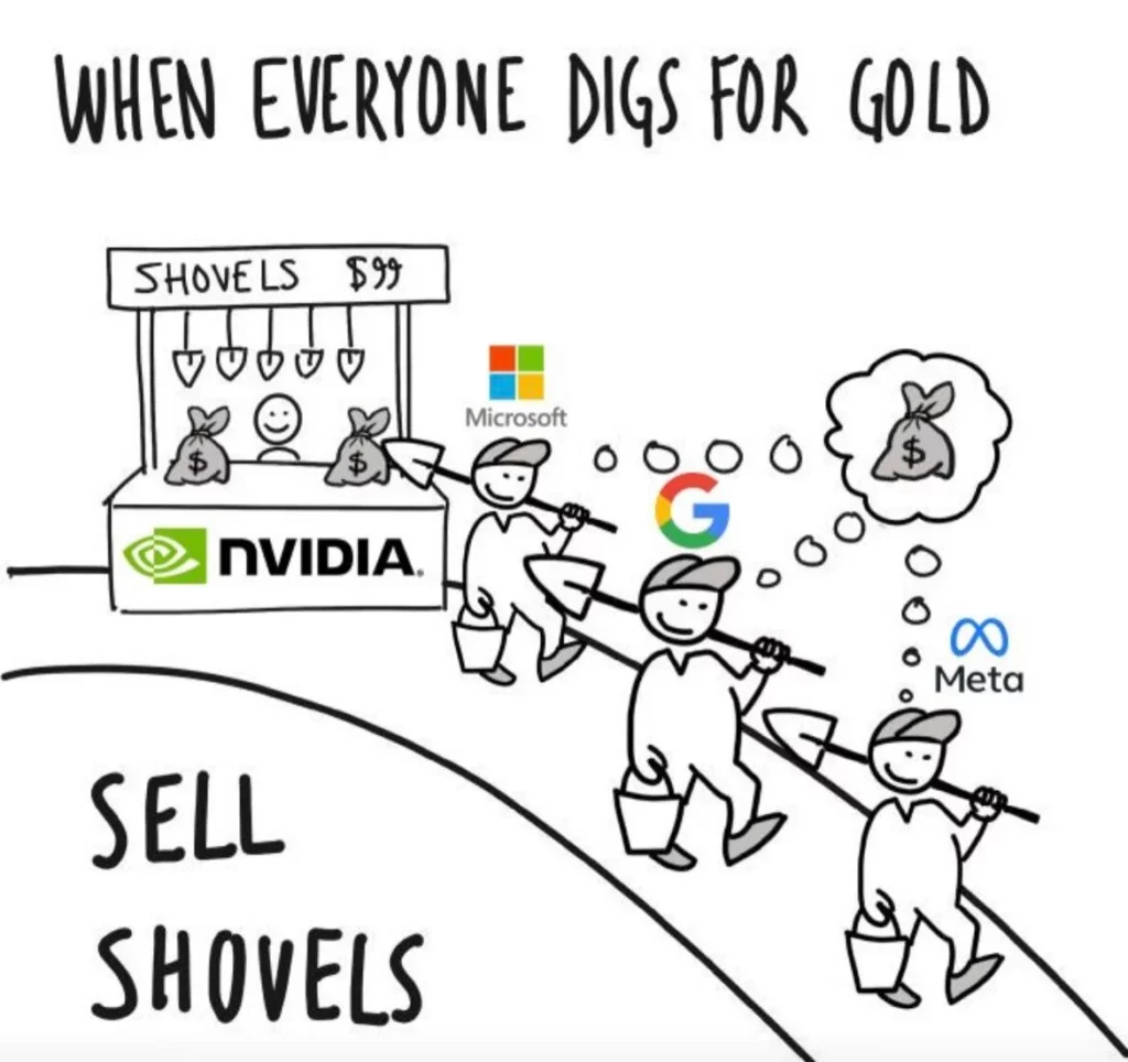
True fortunes aren’t just being made by those building AI applications but by the companies selling the “shovels” – the chips that power every model, experiment, and breakthrough. Just as miners in the 19th century depended on sturdy picks and shovels to unearth gold, today’s AI pioneers rely on GPUs and other specialized AI chips to train and deploy their models. Whether or not a startup strikes it rich with the next killer AI app, the demand for computing power remains constant, making chipmakers the indispensable suppliers of this era’s most coveted resource: processing power. In many ways, the shovels of old have become the chips of today, and those who control them shape the pace and direction of the AI boom.
At the heart of these chips are integrated circuits (ICs), tiny labyrinths of transistors packed into silicon wafers (btw, that’s where the term “Silicon Valley”, VC’s mecca, comes from). They’re engineering marvels, but they come with a vulnerability – an insatiable appetite for electricity.
Cooling the AI Boom
The rise of the AI era directly implicates electricity demand. A study by the Electric Power Research Institute (EPRI) shows that a standard Google search consumes roughly 0.3 watt-hours (Wh), but an AI-powered query like ChatGPT requires closer to 2.9 Wh – almost 10x more. Multiply that by billions of daily queries and you see the scale of the problem. On top of that, inference is just the end-user layer; training the massive models behind those queries requires staggering amounts of computational power. All of this computation generates heat, and keeping data centers cool demands additional energy, creating a compounding effect. The bottom line: AI’s growth curve is directly tethered to power consumption, and whoever solves for efficiency wins.
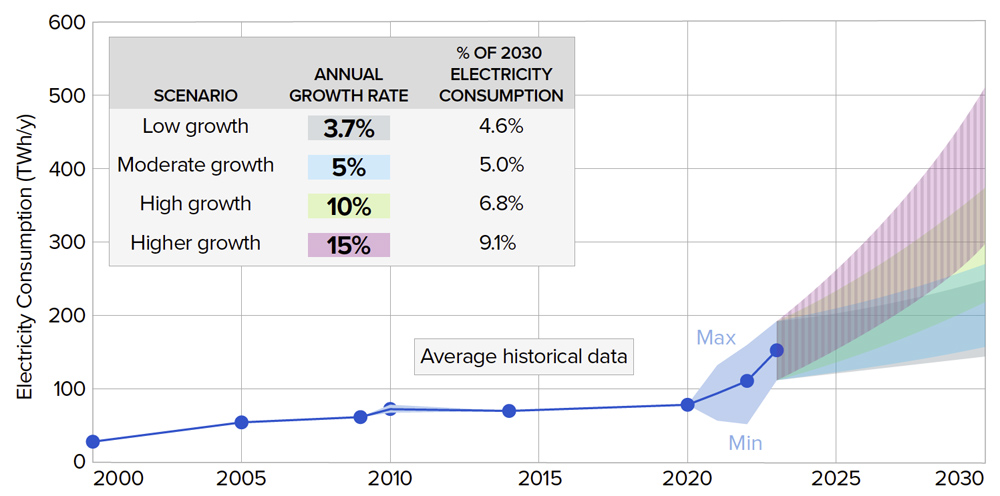
Data centers are quickly becoming the backbone of the global economy, with energy consumption patterns rivaling those of entire countries. This reality strains power grids and accelerates demand for renewable energy infrastructure. But in every constraint lies opportunity: the industry is wide open for innovation in energy-efficient chips.
What Happens When We Can’t Scale Transistors
Computing power is essential for AI development, but the question arises – can we increase it indefinitely? To answer this question, Moore’s Law comes into play. It’s an observation made in 1965 by Gordon Moore, co-founder of Intel. He noticed that the number of transistors on ICs was doubling approximately every 2 years.
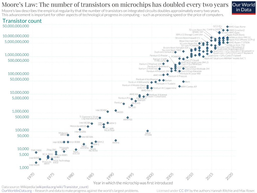
What did it mean in practice? Exponential growth in computing power, falling costs and miniaturization. Chips became more powerful while staying the same size (or even smaller). And as manufacturing improved, the cost per transistor dropped dramatically. This allowed devices to become smaller, more energy-efficient, and drove the widescale adoption of integrated circuits.
However, the number of transistors can’t increase indefinitely. Moore’s Law is slowing down as we are approaching its limitations. There are physical limits – as transistors approach atomic scales, quantum effects such as tunneling (it happens when electrons can pass through the barrier) cause problems. Secondly, as briefly mentioned in the previous paragraph, packing more transistors tightly generates more heat, which is hard to manage. That’s why the industry looks with hope at alternatives such as neuromorphic computing, quantum computing, and optical computing.
Photonic Chips: Yes, But
Concluding the above, it’s clear there’s a growing need for new categories of integrated circuits. Photonic chips stand out as one of the most compelling alternatives because of…
Bypassing transistor scaling limits
Instead of electrons, photonic chips use photons to carry and process information. This means performance can keep improving without depending on ever-smaller transistors, bypassing the slowdown of Moore’s Law.
High bandwidth and low latency
Electrical wires typically carry one signal at a time, but a single optical waveguide can transmit many wavelengths simultaneously (wavelength-division multiplexing, or WDM). This enables thousands of parallel channels where photons move faster and with less resistance than electrons, unlocking ultra-fast communication between chip components, servers, and datacenters – a critical bottleneck in modern AI.
Lower power, less heat
Electronics waste energy as electrons collide with atoms, releasing heat. Photonic chips avoid this by transmitting data with light, resulting in far lower power consumption and dramatically less heat per bit.
New computational possibilities
Beyond communication, photonic chips can also process information directly with light – for example, in optical neural networks – opening the door to faster, more efficient AI algorithms.
…BUT if they are so promising, why aren’t datacenters and AI accelerators already running on light instead of electrons? The answer lies in the challenges of mass adoption.
Logic still belongs to silicon
Photonics excels at data movement and certain math-heavy operations, but general-purpose logic remains easier, cheaper, and denser in silicon transistors.
Integration is complex
Optical systems don’t work alone – they require lasers, modulators, detectors, and electronics to generate, control, and read light. Integrating all of this into a single chip at low cost is only now becoming feasible, and still far from standardized. Making two ecosystems, photonics and electronics, compatible is still a hassle.
The ecosystem isn’t mature
Silicon benefits from decades of optimization, with fabs, supply chains, and design tools honed over trillions of dollars of investment. Photonics is still early, which keeps costs higher and manufacturing less predictable. Packaging can account for up to 80% of all manufacturing costs. On top of that, there’s a notable skills gap – companies are struggling to find employees skilled in photonics.
Market adoption takes time
The first wave of photonic adoption is happening in hyperscale datacenters. For broader adoption the tech needs to prove itself at scale.
In short: photonics shines exactly where today’s AI stacks choke – bandwidth, latency, and power – but mass adoption still hinges on integration, manufacturing costs, and ecosystem maturity. That’s why capital is flowing into teams trying to fill those gaps. The following rounds are a good pulse check on where the market is heading.
Most Notable Recent Rounds in Photonics
Although there are many roadblocks to scaling photonic chips, investor interest is heating up. Below are a few of the most notable recent investments:
- OpenLight (USA, August 2025) secured a $34M Series A to scale integrated photonics for AI data centers.
- Celestial AI (USA, August 2025) raised $255M to accelerate optical interconnects, scaling AI infrastructure with Photonic Fabric technology.
- Q.ANT (Germany, July 2025) raised €62M Series A financing round to accelerate the commercialization of its energy-efficient photonic processors for AI and high-performance computing (HPC).
- Arago (France, July 2025) closed a €22.1M seed round to scale its photonic processor “JEF”, targeting 10× lower energy usage compared to leading GPUs.
- PsiQuantum (USA, March 2025) secured $750M at a $6B valuation to build a fault-tolerant quantum computer using photonic chips.
- Ayar Labs (USA, December 2024) raised $155M series D to accelerate high volume manufacturing of in-package optical interconnects.
- Lightmatter (USA, October 2024) raised $400M Series D, reaching a $4.4B valuation, to deploy its Passage photonic interconnect platform in AI data centers.
My Investment Take & Closing Remarks
I believe photonic chips are an interesting bet because:
- The current hurdles are solvable with funding and time. Packaging and electro-optic integration are the big brakes. In PICs, packaging accounts for the majority of the costs, so winning processes and materials translate directly into unit economics.
- There’s real market depth. Depending on definitions, forecasts point to around $36B by 2030 for optical interconnects and up to $9.65B by 2030 for silicon photonics. Looking at the semiconductors market size, it could even be bigger than we imagine.
- No clear category winner yet. Headlines from the big guys (Nvidia, Intel, Apple, TSMC, and others) show momentum, but the field remains open for new players.
- Alternatives are further out. Neuromorphic and quantum computing will matter, but photonics fixes today’s problems on nearer time horizons.
- The trend is strengthening. AI is pushing copper to the limits; roadmaps point to photonics.
- Plenty of ground to win. Cost-down levers remain in packaging, co-package optics, standardized Process Design Kits, and supply chains – all under-mature.
What I’m looking for (as a VC):
- Defensible IP or tech moat.
- Teams that blend knowledge of photonics and experience in scaling deep tech projects. Great minds and fast executors.
- Proof of demand – successful PoCs or first LoIs.
- Clear product and operations roadmap.
- Own thesis on removing today’s bottlenecks.
Whether you are an early-stage founder building in photonics or a deep tech investor, and you feel like we might have common interests – reach me anytime.
If you are interested in photonics, optical computing, or computing in general, I highly recommend checking out Future of Computing for some good reads and interviews.